v6502demo
Recovered visual6502.org wiki - beta release
RCA 1802E - VisualChips
RCA 1802E
From VisualChips
The RCA 1802 was a pioneering CMOS microprocessor.
See our main site for some more information and images.
Not only was the C2L CMOS process simpler, denser and faster than previous ones, it lends itself to radiation-hard chips, which led to this CPU being found in various space probes. (The bulk silicon process used for our RCA 1802 is not as radiation tolerant as the later silicon-on-sapphire processes, but it was better than other contemporary processes.)
As it happens, it’s also a great process for us to photograph and analyse, because the N and P structures show as different colours, and the layout is very readable. For the same reason, with this chip reverse-engineering the die photo may be feasible without needing to strip the metal.
Contents
- Control Logic
- Datapath
- 1. /ARO, /ALO
- 2. REGWL, REGWR
- 3. /REGRL, /REGRR
- 4. /EF1234, SELREG0, SELREG2, and REGSEL
- 5. DEC, COUT, CIN
- 6. REG_DB_EN, REG_OUT_EN
- 7. NOUTEN
- 8. /LD_IN, /N_TO_RAB, /IN_RESET, INTDB0~INTDB7
- 9. /SET_P1X2, /P_RAB_OUT, /X_RAB_OUT, /LD_X, /LD_P, LD_FR_DB, LD_FR_N
- 10. /LD_T_FR_PX, LD_T_FR_PX, /T_OUT_EN
- 11. /D_ZERO, D_SHIFT_IN, /D_SHIFT, D_OUT_EN, D_SHIFT_OUT
- 12. B_SHIFT_OUT, B_OUT_EN, /B_SHIFT, /LD_B
- 13. EXT_DB_IN, EXT_DB_OUT
- Simple logic gates
- NOR4 layout
- Resources
Control Logic

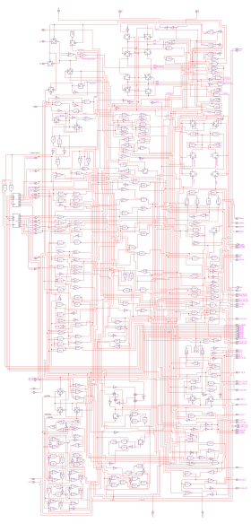
This schematic was derived by tracing the excellent die photo, so the arrangement of the gates pretty much follows the layout on die. There are an extensive use of transparent latches of various enable and output polarities, which are denoted with squares.
The design is much more asynchronous than the 6502 or any of the later CPUs; the clock input at the far left goes through the wait/pause/reset logic, and basically only 2 blocks get clocked at the input rate, which is the signal coming out of U77: the sequencer, and the ALU.
The sequencer is a Johnson counter that uses latches, generating 8 phase-shifted signals I’ve named seq0 through seq7. It’s located southeast of /tpa. Interestingly there’s a patent (6020770) by Motorola several decades later on using transparent latches in a Johnson counter. Anyway, seq0-7 feed the logic to the right, which produces signals active for various periods of the sequence - I’ve denoted these CL0-F. As it’s a latch-based design both rising and falling edges of the clock are used.
The ALU in the bottom left is serial and multiplexer-based. 3 latches above it pick off the lower 3 bits of the internal data bus to select the function. U123 is the main output (goes to D_SHIFT_IN of the datapath), and U63 is the carry out which goes to the carry flag latch U177.
North of the ALU, above the internal databus and below the clock/reset logic, is instruction decoding, fed from the 2-to-16 decoder to its left. Each line of 16 opcodes is decoded separately.
On the east, below the seq0-7 logic, is the main state machine with 4 latches for EXECUTE, INTERRUPT, FETCH, and DMA. Below that are latches for Q and the interrupt enable, as well as more datapath control logic. Finally, the top left corner contains the interrupt/DMA input circuitry.
[text contributed by AmyK]
See #Resources for more.
Datapath

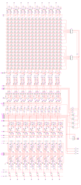
Note that the register bits are just represented as transparent latches, in reality they are two inverters and NMOS transmission gates. But otherwise everything else should be a mostly accurate representation of the circuit.
1. /ARO, /ALO
Located above the register file are a set of latches that drive the address pad outputs. Since the processor can output either the upper or lower 8 bits of any register, these latches have two inputs and two enable signals; ALO and ARO, when asserted, respectively allow the left or right 8 bits of the selected register to be output, and latch the value when deasserted. Taking the leftmost (A7) address latch as an example, we see the storage loop formed by U1, U22, U23, and U20, with the left and right bits entering via U3 and U28 respectively and their gates U2 and U24. When both control signals are deasserted, the loop is closed to latch the last input value, but either of them can be asserted to break the loop and allow either bit’s value to enter.
(Note that in the control logic schematic these are labelled /AHO and /ALO; the inconsistency is because which half of the register file held which bits was not yet known before deciphering the control logic.)
2. REGWL, REGWR
When asserted, these signals cause the respective bit line to be driven via the inverted data-in signal coming from the logic below, to effect register writes. This is shown in the schematic for the leftmost bit as the controlled buffers U4 and U62, and the data-in signal via U64. The storage element of the register file is the standard inverter loop with NMOS pass transistors, and writing is usually accomplished by forcing the bit to the right value, as the bit lines have a stronger drive than the storage inverters. The datapath analysis athttp://home.earthlink.net/~schultdw/1802/datapath/index.html suggests that the large rectangular series PMOS transistors in the middle disconnect power to the PMOS inverters in the storage loop during a write, although this would mean the 1802 is not truly static since stopping the clock when either of these control signals is high would result in data loss.
3. /REGRL, /REGRR
These signals control the latch between the register output and the increment- decrement unit. With asserted, the respective 8-bit half of the register chosen are output into the incdec, and the output is latched once deasserted. Taking the leftmost element as an example again, the storage loop is formed from U9, U70, U10, and U73, with entrances via U7/U8 and U65/U67. Notice that the write data line goes up through the middle of this latch unit in the IC layout.
4. /EF1234, SELREG0, SELREG2, and REGSEL
Not part of the datapath proper, but these signals run horizontally through it, to the circuitry to its right. /EF1234 is an input of the value on the selected /EF{1,2,3,4} input. SELREG0 resets all the register selection latches, causing register 0 to be selected, while SELREG2 has the same effect as well as setting bit 1 of the register selection bus, causing register 2 to be selected. REGSEL loads the register selection latches from the register address bus (RAB).
5. DEC, COUT, CIN
Output from the register file enters the incdec, which can optionally increment or decrement the data going through it using transmission-gate XOR logic. The CIN signal provides the carry in, COUT carries out, and DEC allows the circuit to decrement. The ripple carry chain is of the common alternating type, used to reduce gate delay and transistor count by interleaving NOR with NAND.
6. REG_DB_EN, REG_OUT_EN
These control two transmission gates between the vertical databus, incdec output and register write input. Their operation can be summed up as follows:
REG\_DB\_EN REG\_OUT\_EN   Description
   0         0            Registers disconnected; inactive
   0         1            incdec output can be written to a register
   1         0            Databus can be written to a register
   1         1            A register can be output to databus and also written back
7. NOUTEN
This is another signal which is not part of the databus proper but only enables output of N0, N1, and N2 from the lowest 3 bits of the IN databus.
8. /LD_IN, /N_TO_RAB, /IN_RESET, INTDB0~INTDB7
The first loads the I and N registers from the vertical databus. Like all the other registers in the 1802, I and N are implemented using transparent latches, so their values are latched once /LD_IN deasserts. For bit 7 (bit 3 of I), the storage loop consists of U16, U92, and U89. They continuously output on the IN databus, INTDB0~INTDB7. The /IN_RESET signal clears both I and N to 0, while /N_TO_RAB causes N to be output to the internal register selection bus too.
9. /SET_P1X2, /P_RAB_OUT, /X_RAB_OUT, /LD_X, /LD_P, LD_FR_DB, LD_FR_N
Below the IN databus are the X and P registers, with X on the left and P on the right. Each register consists of a resettable or settable latch, depending on bit position; the /SET_P1X2 signal makes use of these differences to set P to 1 and X to 2 when it is asserted. /P_RAB_OUT and /X_RAB_OUT gate these registers onto the register address bus where their values can be latched in the register selection logic using REGSEL (see above) or the other register, via the /LD_X, /LD_P, and LD_FR_N (should actually be LD_FR_RAB) signals. LD_FR_DB allows the loading of X and P from the vertical databus. Note that asserting both LD_FR_DB and LD_FR_N connects the vertical databus to the RAB, although conflicts will occur due to the differing bit widths.
10. /LD_T_FR_PX, LD_T_FR_PX, /T_OUT_EN
Immediately below X and P is the 8-bit-wide T register. T can only be loaded to from X and P, via LD_T_FR_PX and its inverse. It is only output to the vertical databus, accomplished by assertion of /T_OUT_EN.
11. /D_ZERO, D_SHIFT_IN, /D_SHIFT, D_OUT_EN, D_SHIFT_OUT
These signals are related to the D register, one slice (bit 7) comprised of the components U110 through U120 in the schematic. /D_ZERO is an output, indicating when all of the bits of D are zero, accomplished by a chain of NAND gates with one inverted input (the rightmost bit has instead an inverter, U919.) It can be seen that the structure has two storage loops, which for bit 7 comprises U112, U113, and U114 for the first, and U115, U117, and U119 for the second. The two loops are connected such that the first is closed when the second is open, and vice-versa, controlled by the /D_SHIFT signal. This forms a master-slave edge- triggered flip-flop, of which 8 are connected in a shift register arrangement. On each negative edge of /D_SHIFT, one bit is shifted into the register via the D_SHIFT_IN input, and another out via D_SHIFT_OUT. D_OUT_EN outputs D onto the vertical databus with asserted. Notice that this means D cannot be loaded from the databus directly, but each bit must be shifted in via the D_SHIFT_IN input. D is a serial in/out, parallel out right-shifting register.
12. B_SHIFT_OUT, B_OUT_EN, /B_SHIFT, /LD_B
The B register is similar to the D register, but there are two differences: the shift input, instead of having a B_SHIFT_IN signal, is permanently grounded so that only 0 bits can be shifted in, and there is the ability to load it in from the databus in parallel, by asserting /LD_B. B_SHIFT_OUT and B_OUT_EN are same as for D, but /B_SHIFT has to be maintained at a low level in order for /LD_B to load the B register, whose main storage loop is U127, U129, U130, and U131 (the lower transparent latch) for bit 7. The upper latch, consisting of U122, U123, and U124, remains transparent except during a shift. Thus, to clear B, it can be done by applying 8 positive-going pulses to /B_SHIFT; to load B from the vertical databus, assert /LD_B, and deassert it to latch the value in the lower transparent latch. Then its bit 0 appears at B_SHIFT_OUT, and successive pulses on /B_SHIFT will shift bits out to the right and zeroes in from the left.
13. EXT_DB_IN, EXT_DB_OUT
These signals are straightforward to understand: they control the interaction between the vertical databus and the external pads. EXT_DB_IN enables the value of the respective databus bond pad to be driven on the vertical databus via a controlled buffer, while EXT_DB_OUT outputs the signal on the vertical databus.
Simple logic gates

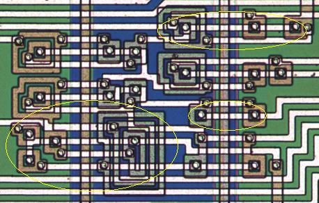
Above we see a detail of our high-resolution images, showing several logic gates laid out with their complementary pullup and pulldown trees in their respective areas (Orange on green is NMOS, purple on blue is PMOS.) The power supply to each gate is the substrate (or well) so there are fewer contacts than in the usual technologies.
Middle-right is the simplest gate: an inverter, with a single pull-down and single pull-up. Above it is a 2-input NOR gate and to the left is a 3-input NOR gate. The three concentric transistors of the NOR3 are rarely seen on this chip, perhaps because of the reduced drive and speed of having 3 transistors in series.
NOR4 layout
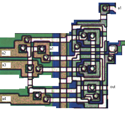
If a NOR4 were laid out like the NOR3 above, it would be rather large because of the need for 4 concentric transistors. The largest (outside) transistors would present more load to their drivers, but wouldn’t contribute more drive to the NOR4 because that will be limited by the innermost transistor.
So here we see an alternative layout technique, where an isolated region is created in the lower right, containing two of the pullups, the upper one of which is operated inside-out.

Resources
- The CPUs of Spacecraft Computers in Space
- RCA 1802 on wikipedia
- Manuals at decodesystems.com and at bitsavers
- A high speed bulk CMOS CCL microprocessor (abstract only)
- A Radiation-Hardened Bulk si-Gate CMOS Microprocessor Family paper
- C2L: A new high-speed high-density bulk CMOS technology (abstract only)
- RCA’s Sarnoff Center archives
- Milestones That Mattered: CMOS pioneer developed a precursor to the processor 2006 EDN retrospective
- COS-MOS Could Put Computer Slice on a Chip 1970 EDN article
- conventional CMOS NAND gate in wikipedia.
- RCA COSMAC 1802 on The Antique Chip Collector’s Page
- Galileo spacecraft computer on wikipedia
- Galileo - True distributed computing in space on Computers in Spaceflight: The NASA Experience website
- Emma 02 emulator by Marcel van Tongeren, source available for non-commerical use. Some copyright by Michael H Riley and others.
- The 1802 Cosmicos Single board computer by Bob Stuurman of Radio Bulletin (website by Hans Otten)
- David Schultz’s analysis of the layout and circuits
- Chuck Bigham’s simulation of the control logic
- One of several discussion threads in Yahoo “cosmacelf” group
Retrieved from “http://visual6502.org/wiki/index.php?title=RCA_1802E”